-
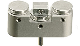
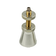
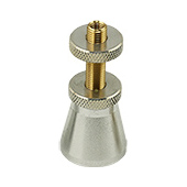
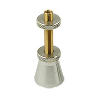
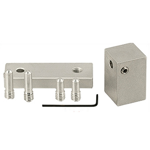
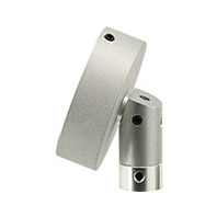
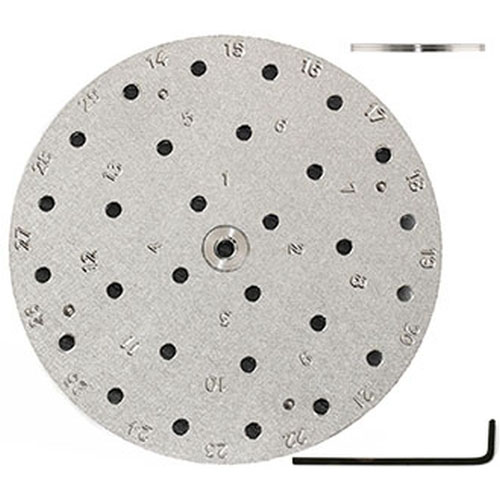
EM-Tec FS21 combines the EM-Tec F12 FIB grid holder with two standard 12.7mm (1/2) pin stubs. The F12 FIB grid holder and the sample stubs can be rotated in the holder for selecting the optimum orientation in the FIB/SEM system. The EM-Tec FS21 FIB grid and sample holder enables loading the samples and FIB grids close together. The FIB grid and the sample stubs are at the same level when using Si wafer samples
-
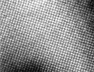
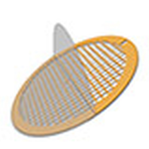
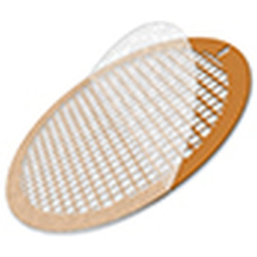
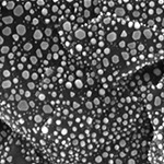
Oriented gold crystal provides plane spacing of 0.102, 0.143 and 0.204nm. Used for checking resolution, image quality, magnification and instrument stability in high resolution TEMs. The single oriented gold crystals produces a characteristic diffraction patterns. When the TEM is correctly setup, it should resolve the 0.102 nm (100 plane) planar spacing, 0.143 nm (220 plane) and the 0.204nm (200 plane). Since these are physical constants they can also be used for magnification calibration. Mounted on a 400 mesh Au TEM grid.
-
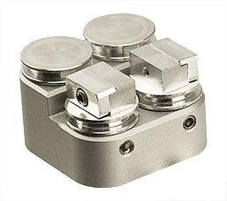
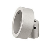
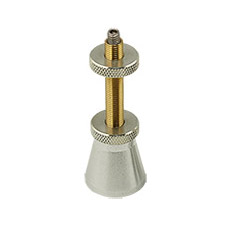
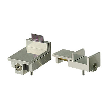
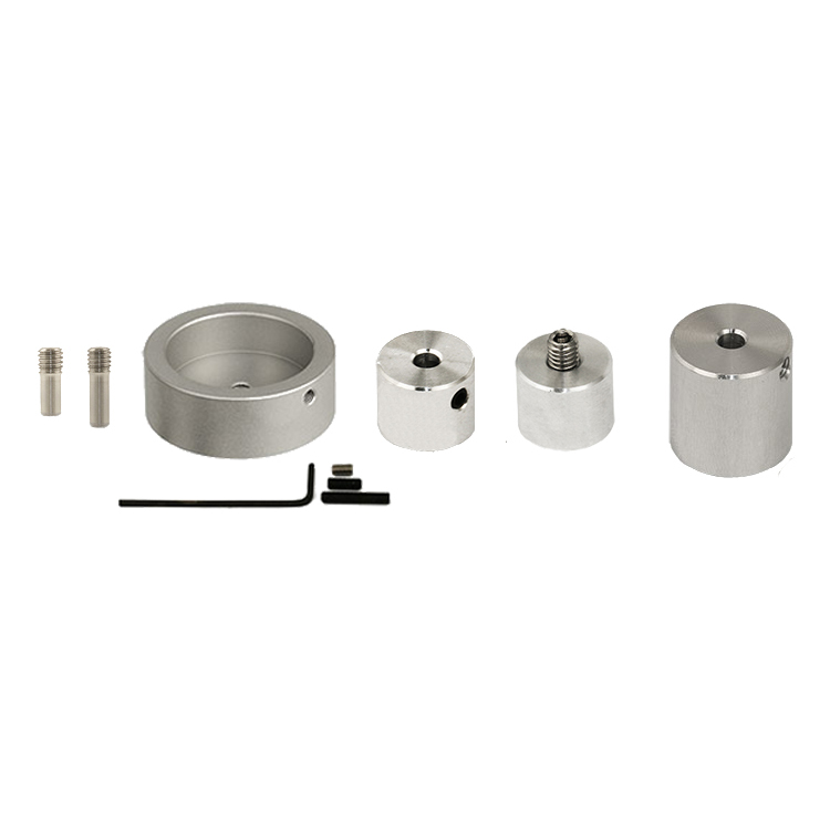
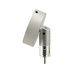
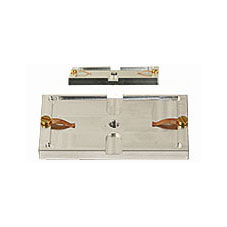
EM-Tec FS22 combines two F12 FIB grid holders with two standard 12.7mm (1/1) pin stubs within a 27x27mm footprint. Both the F12 FIB grid holders and the pin stubs can be rotated independently in the holder for selecting the optimum orientation in the FIB/SEM system. The EM-Tec FS22 dual FIB grid and sample holder enables loading the samples and FIB grids close together. The FIB grid and the sample stubs are at the same level when using Si wafer samples.
-
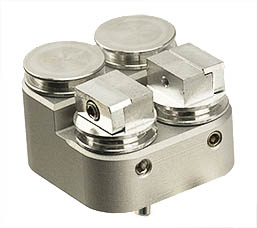
EM-Tec FS22 combines two F12 FIB grid holders with two standard 12.7mm (1/1) pin stubs within a 27x27mm footprint. Both the F12 FIB grid holders and the pin stubs can be rotated independently in the holder for selecting the optimum orientation in the FIB/SEM system. The EM-Tec FS22 dual FIB grid and sample holder enables loading the samples and FIB grids close together. The FIB grid and the sample stubs are at the same level when using Si wafer samples